Precision in Every Step. Performance in Every Cell
Explore the advanced manufacturing processes and technologies behind Indosol’s solar wafers, cells and modules. Discover how each stage of production contributes to quality, efficiency and reliable performance across the solar value chain.
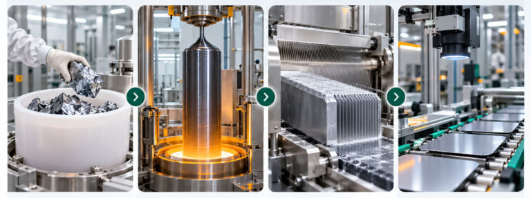
A solar ingot is a cylinder of high-purity crystalline silicon. We grow ours by the Czochralski (CZ) process: purified polysilicon is melted at very high temperature, a seed crystal is lowered into the melt and drawn upward slowly, and the silicon solidifies as one continuous n-type crystal.
With recharged Czochralski (RCz) pulling, the crucible is refilled between pulls so several ingots are grown from one crucible. The ingot is then squared and sliced by diamond wire into ultra-thin wafers, the semiconductor substrate on which the cell is built.
Process flow
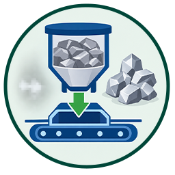
Polysilicon charging
Each lot is recorded and traced through the plant.
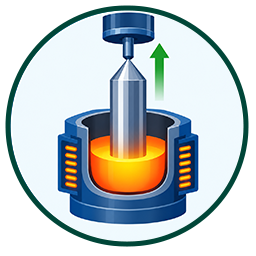
RCz ingot pulling
A single n-type crystal is drawn from molten silicon.
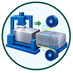
Squaring and diamond wire slicing
The ingot is squared into bricks and sliced into wafers.
Inspection and sorting
Every batch is inspected electrically and geometrically.
Precision at Every Step. Purity in Every Wafer
Recharged CZ pulling
Several ingots per crucible, for lower energy consumption per kilogram of silicon.
Advanced heat shield
A controlled thermal profile around the growing crystal, for low defect density.
Lot-level traceability
Documented polysilicon origin carried from feedstock through ingot to wafer.
One-touch automated crystal growth
Even dopant distribution and minimal radial resistivity variation across the ingot.
Carbon and oxygen control
Optimized C/O concentration in the crystal, which supports higher cell efficiency.
Advanced diamond wire slicing
Uniform thickness, low micro-crack formation, high mechanical strength and minimal material loss.
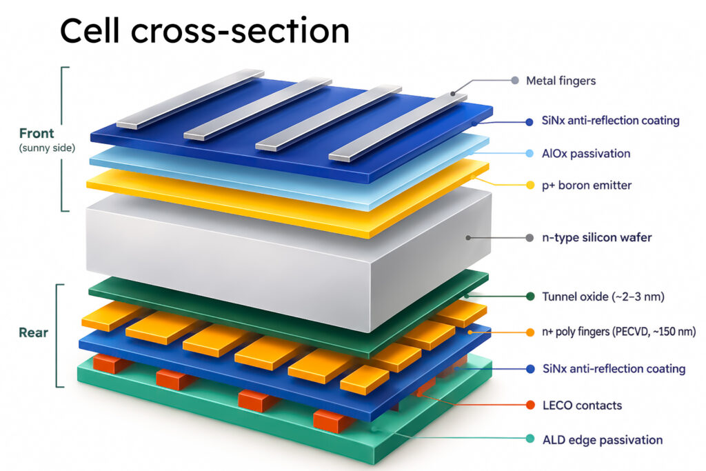
TOPCon (Tunnel Oxide Passivated Contact) is the n-type cell architecture replacing conventional PERC. An ultra-thin tunnel oxide layer and a doped polysilicon layer at the rear allow current to flow while minimizing recombination at the contact. The cell is bifacial, generating electricity from both sides.
Our TOPCon+ architecture adds four process steps to this platform.
Rear poly-finger
In a standard TOPCon cell the polysilicon covers the whole rear and absorbs light. We keep it selectively beneath the metal fingers, reducing parasitic absorption and improving rear-side response and bifaciality.
Uniform ALD edge passivation
Cutting a cell into half cells exposes bare silicon at the cut edge. A conformal ALD film passivates those edges, reducing perimeter recombination.
Engineered poly interface
Phosphorus-doped PECVD polysilicon over the tunnel oxide, engineered for lower reverse current and improved shade resistance.
Laser-enhanced contact optimization (LECO)
A laser step after firing forms the front contacts at fine, localized points, for lower contact resistivity and higher open-circuit voltage.
Technology Roadmap
AT START
TOPCon+
25.5%
LECO, edge passivation and polyfinger metallization.
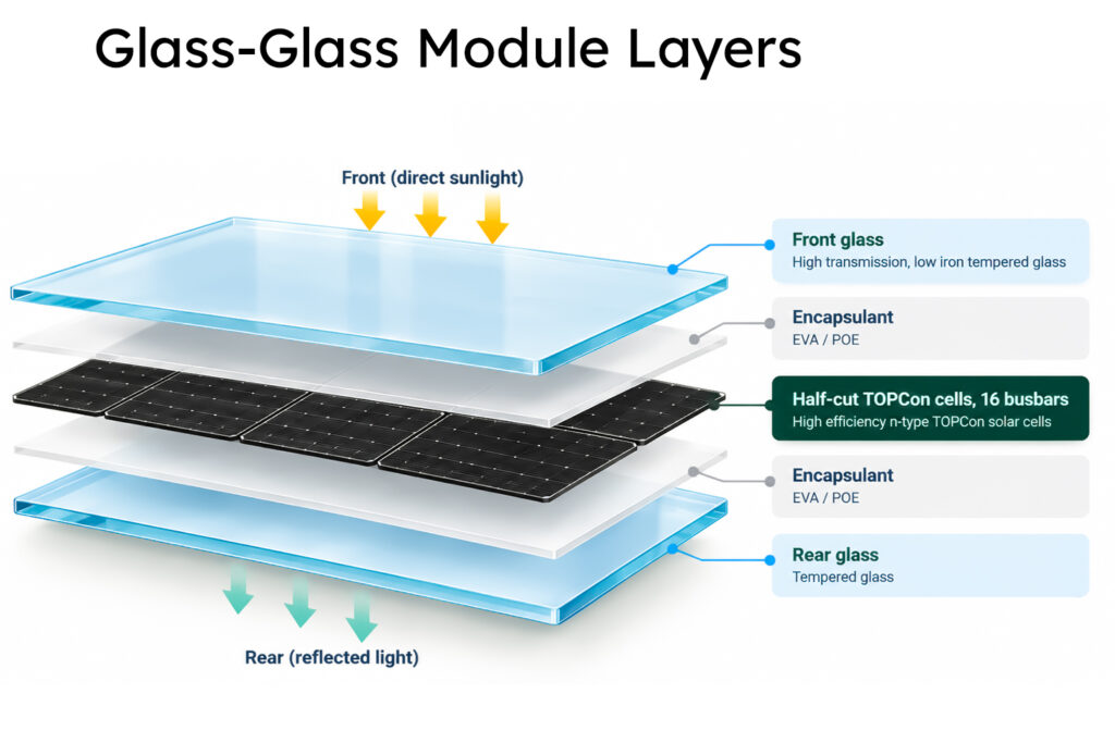
A module has to deliver the cell’s performance outdoors for decades. Four construction choices do that work.
Half-cut cells
Each G12R cell is cut into two, halving the current each cell carries. That lowers resistive losses and reduces the effect of partial shading and hotspots.
16-busbar interconnection
More, finer busbars shorten the path current travels across the cell and keep it collecting even if a micro-crack forms.
Glass-glass construction
Glass on both sides seals the cells against moisture and supports them evenly under load, for structural crack tolerance and PID resistance.
Bifacial design
The transparent rear lets the cell use light reflected from the ground, adding to energy yield beyond the front-side rating.
Indosol REAL™ – G12R N-Type TOPCon Bifacial Solar Module